The Engineering Research Center for Semiconductor Integrated Technology is an advanced technology platform for optoelectronics, microelectronics and MEMS. It was constructed by the Institute of Semiconductors, Chinese Academy of Sciences in 2002 for its strategic development. All the advanced facilities for semiconductor key processes and measurements are worth over 130 million RMB. The working area includes 1,700 m2 in the clean rooms and 1,100 m2 in the offices and test rooms. With the progress of the standard of service and management, the center has become the critical technical support department for research, student training and technique exchanges.
The key processing equipment in the center includes an E-beam lithography system, a laser direct writing system, a nano-imprint system, an MA6/BA6 double-side mask aligner and EVG mask aligner, an inductively coupled plasma (ICP) etching system for Si, SiO2, metal and III-V semiconductors, an E-beam evaporator, an ion beam sputter for optical film, a magnetron sputter, a plasma enhanced chemical vapor deposition (PECVD) system, a low-pressure chemical vapor deposition (LPCVD), an ion implantation system, a thermal oxidation system, a metallization system and a wafer bonding system. The primary measurement equipment includes a scanning electron microscope (SEM), a focused ion beam system (FIB), a spectrophotometer, a surface profiler, a low temperature probe station, a network analyzer, a semiconductor device analyzer, a MEMS stability and spectrum testing system and a solar cell I-V/QE measurement system.
The center is an open platform, offers not only technical services and project cooperation, but also technology consulting services for researchers. In order to effectively provide technical support and equipment, the center has joined many technology platforms of public service, e.g. the Technology Joint Platform of Institutes in the Chinese Academy of Sciences, the Nano-apparatus Platform of the Knowledge Innovation Engineering Base in the Chinese Academy of Sciences, the Beijing Regional Center of Information Electronic Technology Instruments, the Capital Science and Technology Platform, and the Zhongguancun Science Park Open Lab.
Prof. LU Yongxiang, former president of the Chinese Academy of Sciences, visited the Institute of Semiconductors, CAS on August 28, 2006. He said: “The advantage of the Institute of Semiconductors is the combination of optoelectronics and microelectronics. The institute should further improve the ability of independent innovation and integrated technology, pushing the construction of the technical platform. The Engineering Research Center for Semiconductor Integrated Technology, constructed two years ago, has equaled to the abovemiddle level of European technical centers. Both equipment and the working environment are so good that the strong core competitive advantage has been formed for the third period innovation plan. Next, the platform might contribute to national scientific and technological innovation, being open to other institutes. The establishment of the center shows that the leadership group has strong judgment ability, progressive ideas and decision-making ability. It also shows the strong supports of all employees to the wise policy decisions of the leadership group.”
The aim of the center is continually improving the level and the ability of semiconductor technology to satisfy the scientific needs of the institute, to develop the information technology to meet the major national needs and the national economic development, to make breakthroughs in pivotal and reliable technology to accelerate the transfer of research achievements, and to be opened to the outside as a top technical center for student training, academic cooperation and communication.
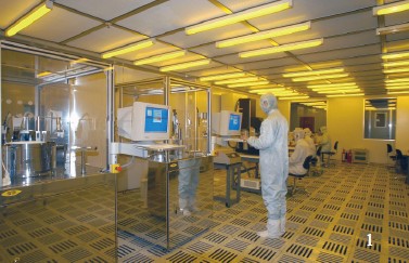
1 10-class photolithography room
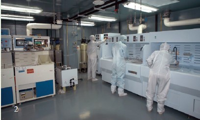
2 Cleaning/etching room
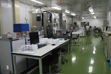
3 Plasma enhanced chemical vapor deposition system /Inductively coupled plasma etching system
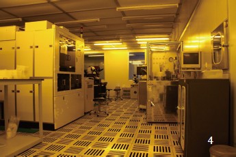
4 Micro-electronic processing line
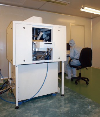
5 E-beam lithography system