The Nano-Optoelectronics Laboratory focuses on research about semiconductor optoelectronic materials and devices. The lab has made breakthroughs in the research of quantum well lasers, and made key contributions to the development of quantum well lasers with multiple wavelengths realized by different material systems for various applications. It has received 3 first-grade "Awards for Science and Technology Achievements of CAS", 2 second-grade and 2 third-grade "National Awards for Science and Technology Achievements".
With the development of optoelectronic devices towards smaller size and lower dimension, the nanostructures demonstrate many novel quantum phenomena and effects with rich physical properties, which are utilized to develop optoelectronic devices with novel functions. According to the principle of "Innovation, progress and continuous development", and based on previous R&D work, the lab’s research is focusing optoelectronic materials and devices oriented. Apart from optical communication applications, the lab is especially interested in the applications of nano-optoelectronic technology in the fields of optical storage, optical displays, optical information processing and laser related bio-medical applications.
The lab has a research team that includes more than 50 researchers, mainly consisting of young investigators. At present, the lab has 1 CAE academician, 7 full professors , 5 associate professors, 15 assistant professors and technicians, 3 postdoctoral researchers, and more than 20 graduate students. Under the guidance of Prof. CHEN Lianghui, an academician of the CAE, the lab is now funded by the "863", "973"National Research projects, the National Natural Science Foundation of China, and CAS.
The lab is equipped with advanced facilities for material growth, characterization, and device processing. The lab closely cooperates with many prestigious overseas universities, research institutions and industrial organizations. With research on nano-optoelectronics science and technology, the lab seeks to be a respected research center for semiconductor nano-quantum materials and devices, an incubation center for novel devices and technologies, and a cultivation center for talented researchers.
Research direction
Low-dimensional semiconductor material growth and studies of growth kinetics/dynamics.
Quantum well lasers, vertical cavity surface emitting lasers, and quantum dot lasers.
Quantum well/dot infrared photodetctors and the focal plane arrays.
Antimonide-based lasers and detectors.
GaN based light emitting diodes and lasers.
Surface plasmons, near field optics and near field optical sources.
High power lasers and failure mechanism analysis.
Key optoelectronic device processing technology.
Reseavch on inovganic stretchable and flexible optielectroies.
Research Equipment
The lab is equipped with advanced facilities for material growth, device processing and characterization/analysis systems.
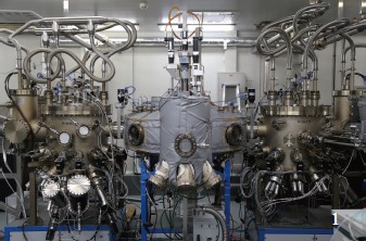
1 Molecular beam epitaxy (MBE) system
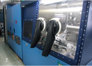
2 Metal organic chemical vapor deposition MOCVD
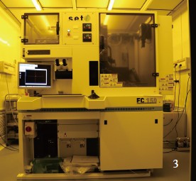
3 Device Bonder FC150
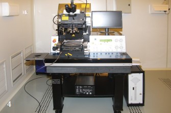
4 Mask Aligner(Suss MA6)
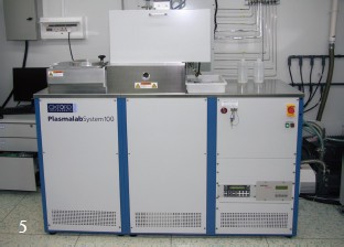
5 Inductively coupled plasma (ICP) system

6 Field emission scanning electron microscope(SEM)
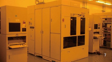
7 Stepper
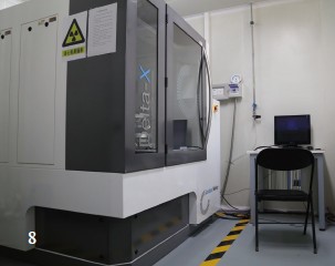
8 X-ray double Crystal Diffraction system