The Key Laboratory of Semiconductor Material Science (LSMS), affiliated with the Institute of Semiconductors, Chinese Academy of Sciences (CAS), is one of the leading research laboratories in China, specializing in advanced semiconductor material science and device technologies. Under the guidance and leadership of Prof. Lin Lanying and Prof. Wang Zhanguo, both members of the Chinese Academy of Sciences, the laboratory was established in 1990.
LSMS research spans both applied engineering technologies and fundamental studies of basic semiconductor material sciences and device physics, including low-dimensional quantum well/wire/dot materials and devices, high performance semiconductor lasers and integrated photonic chips, quantum cascade lasers, wide bandgap semiconductor materials and devices, microelectronic materials and devices, organic and inorganic composite materials, photovoltaic materials and technologies, diluted magnetic materials, and space microgravity material growth technologies. The laboratory conducts research in both the fundamental semiconductor materials science and high performance photonic semiconductor devices with commercial applications, providing small volume engineering samples and per-commercial technology incubation. In accordance with the China's national strategy of invigoration through investment in science and education, LSMS pursues a long term roadmap with the goal of establishing the laboratory as both a top ranking research center domestically, and also an internationally influential laboratory in advanced semiconductor materials and device technologies. Simultaneously LSMS is tasked with the mission of providing a high quality graduate level education for the next generation of scientists and engineers in the field.
Research Direction
Low dimensional semiconductor material and devices, including self organized quantum dots, quantum cascade lasers, two-dimensional crystalline materials, organicinorganic composite materials and devices.
Photonic Integrated Circuit (PIC) material engineering and devices.
Wide bandgap semiconductor materials and devices.
Novel photovoltaic materials and applications.
Low-dimensional semiconductor material physics and surface/interface engineering.
InP, GaSb, InAs and novel single crystal semiconductor material growth and substrate fabrication technology.
Research Equipment
The laboratory is well equipped with a wide range of state-of-the-art equipment for advanced material growth, including molecular beam epitaxy, metal-organic chemical vapor deposition, ion beam epitaxy, and magneto-sputtering systems. Additionally, the laboratory is equipped with multiple advanced systems for material quality analysis and metrology studies, such as an Fourier transform infrared spectrometer, scanning probe microscopes, photoluminesecence systems, Raman spectroscopy, reflectance difference spectroscopy, Hall-effect measurement system, deep-level transient spectroscopy, and electro-chemical C-V measurement systems.
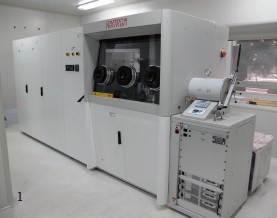
1 MOCVD system
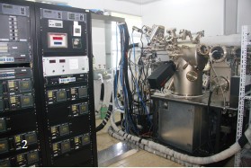
2 Molecular Beam Epitaxy System
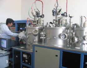
3 Double-ion-beam assisted deposition and plasma etching systems
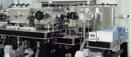
4 Deep ultraviolet laser photoluminescence spectrometer

5 Fourier transform infrared spectrometer
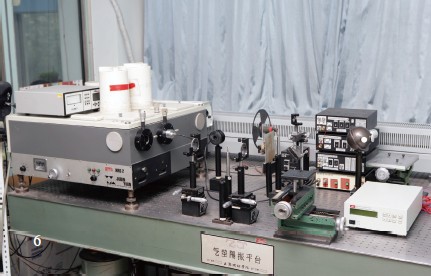
6 Spectrum measurement system and scanning probe microscope