The National Engineering Research Center for Optoelectronic Devices (NERC-OED), with the assistance of the National Development and Reform Commission (formerly the National Planning Commission), is organized by the Institute of Semiconductors, Chinese Academy of Sciences (ISCAS) in order to meet the rapid development needs of China’s optoelectronic industry and to meet the needs of domestic and oversea markets for optoelectronics. NERC conducts engineering research for identified key optoelectronic devices, and provides core technologies, general technologies and processing technologies for China’s optoelectronic industrialization development. In December 1996, NERC was formally certificated by the state. In August 1999, Hi-Tech Optoelectronics Co., Ltd. (HTOE) was founded on the basis of NERC’s technology background, retaining NERC as a national research center. The company is operated by the China Energy Conservation and Environment Protection Group (CECEP) and ISCAS.
NERC provides independent technology and a complete process line of semiconductor optoelectronic devices, including material epitaxial growth, chip processing, packaging, and testing and aging of devices. NERC has capabilities of research and development of semiconductor optoelectronic devices and semiconductor functional materials, development and integration of opto-mechatronic systems, development of optoelectronic technologies, undertaking of optoelectronic and electronic projects and optical communication projects, and research and development of a variety of optical devices, sensor technologies and devices and other products.
NERC has established the training points of a Master of Engineering and a Doctor of Engineering program in the specialties of ‘solid optoelectronics and microelectronics’ and ‘physical electronics’, and receives post-doctoral researchers.
Research direction
High-power semiconductor lasers (arrays) and laser modules
High-power lasers and their failure mechanisms
Key technology of optoelectronic devices
Optoelectronic devices used in the industrialization of optical displays
Semiconductor lasers, photodetectors and their arrays used in optical communication
Fiber lasers and their applications
All solid-state lasers and their applications
Optical sensing and broadcasting system and its applications
Research Equipment
The research equipments include: epitaxial growth systems, coating system, packaging systems, testing systems, UV irradiation systems, optical waveguide testing systems.
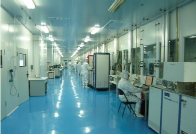
1 E-Beam Facet-Coating Equipment
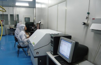
2 Thin film Test System
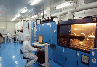
3 MOCVD(metal organic chemical vapor deposition) system
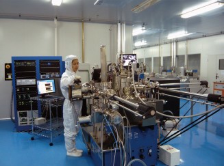
4 Laser diode bar cleaving line
Scientific research products
GaAs/InP-based epitaxial wafers, high-power semiconductor laser single-die and bar chips, single-die COS, single-die devices, arc-shaped, ring-shaped and other irregular shaped packages of 10,000-watt array devices, optical fiber coupling modules, solid-state lasers, etc.
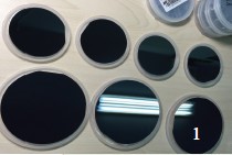
1 GaAs/InP Wafer
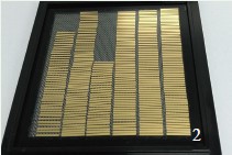
2 Laser Bar Chip

3 COS Packaged Single Emitter Lasers
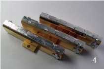
4 CW Laser Array with Linear Package (7×20W)
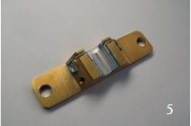
5 Semi-Circular Package
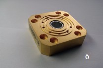
6 Circular Package
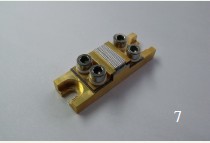
7 Stack packaged Laser Array (0.4mm-Space)
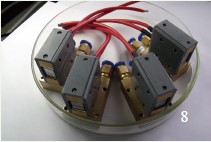
8 Microchannel Stack packaged Laser Array (1.2mm-Space)
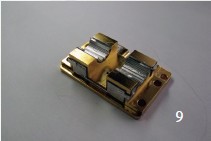
9 Kilowatt QCW Laser Array with Stack Package (2000W)
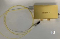
10 100W Mulity-Single Smitters Fiber Coupled Module
