In accordance with national development strategies, SSL R&D Center of CAS was established at the Institute of Semiconductors (IOS), CAS. The center consists of a series of professional R&D platforms, such as the State Key Laboratory of Solid State Lighting, National Center for International Research, Beijing Engineering Research Center for the 3rd Generation Semiconductor Materials and Application, etc. By focusing on the national research plan and project, the SSL R&D center takes the 3rd generation semiconductor materials and devices as the starting point to achieve break-through in key technology of industrialization commonality, which would provide guidance to the SSL and the 3rd generation semiconductor materials, drive the industrial development in microelectronics, optoelectronic materials and devices in the field of information and energy. Meanwhile, promotion of related academic subjects and formation of an independent and innovative talent team can be expected.
Implementation of basic, forward-looking and strategic scientific and technological research, realization of scientific & technical innovation center for the 3rd generation semiconductor materials and SSL.
Launch of research on common and key technologies for industrialization, technical radiation center and industrial service platform to ensure the sustainable development of SSL.
Integration of International resources to become an international cooperation base for the 3rd generation semiconductor materials and SSL.
To develop a world-class technical team in the area of the 3rd generation semiconductor materials and SSL.
Research area
The 3rd generation semiconductor materials
R&D of major equipment (MOCVD)
Material and device study of solid-state light source in ultraviolet range
Study of SSL material and device with ultra-high energy efficiency
Research of novel detector and photovoltaic technology
Novel application of SSL (agriculture, medical treatment and communications)
R&D facility
The SSL R&D Center has setup a complete semiconductor processing line which covers the entire industrial chain such as equipment, materials, chip fabrication, packaging, application and test analysis. The 1500m2 clean room consists of over 200 semiconductor equipment with international standard. The lab is capable of providing comprehensive service to the R&D of the 3rd generation semiconductor materials.
Epitaxy equipment
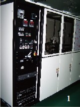
1 MOCVD
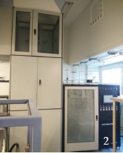
2 HVPE
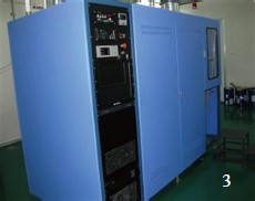
3 HT MOCVD
Chip processing equipment
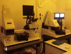
4 Photolithography
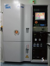
5 E-beam evaporator
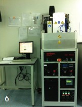
6 PECVD
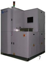
7 ICP刻蚀系统 ICP
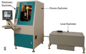
8 Laser lift-off
Test and analysis equipment
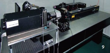
9 PL
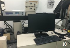
10 Time resolved fluorescence spectrometer
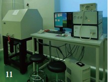
11 Raman spectrometer AFM
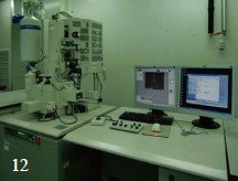
12 SEM
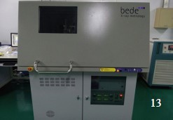
13 XRD
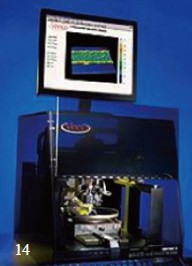
14 Profiler
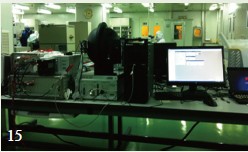
15 T3Ster thermal resistance tester
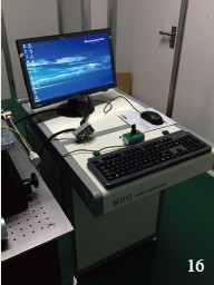
16 Semiconductor discrete device testing system
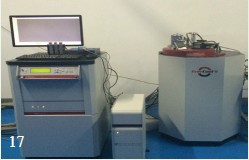
17 EMMS
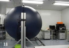
18 LED testing system
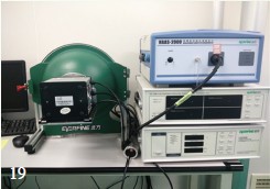
19 Optical power tester for UV devices
