Recently, a study titled "Chemical vapor deposition growth of two-dimensional heterojunctions" by Prof. Zhongming Wei at Institute of Semiconductors, Chinese Academy of Sciences, was published in SCIENCE CHINA Physics, Mechanics & Astronomy. In this review, the methods of chemical vapor deposition (CVD) to fabricate 2-D heterojunctions are explained based on research conducted over the last few years. The developmental history of heterojunctions of 2-D materials is introduced, along with the influences of different growth conditions on heterojunctions. Finally, the study details some other methods to prepare heterojunctions.
The transfer method is a good laboratory technique for heterojunctions of 2-D materials. Researchers can easily utilize this method to obtain the specific heterojunction they want. However, an efficient and stable technique is needed for industry. Chemical vapor deposition is introduced to fabricate heterojunctions as a potential method. The chemical vapor deposition method is sensitive to changes of growth conditions. It is an important research topic to ascertain influences of different factors on the growth process and final heterojunctions. This review classifies the factors into temperature, substrate, precursor, lattice mismatch, carrier gas flow rate, and carrier gas composition.
When any one of factors is changed, the resulting heterojunctions will have different structures or components. These factors also influence each other. So the desired heterojunctions of 2-D materials can't be fabricated simply by modifying one parameter of the chemical vapor deposition system. For example, when different precursors are used, the growth temperature should be reset due to the different evaporating temperatures of different precursors. Besides these, the method through sulfuring patterned films, such as metal films, oxide films and other component films to fabricate heterojunctions is also referred.
Further studies are necessary to solve problems in the fabrication of heterojunctions of 2-D materials. MBE and MOCVD can also be considered as good options of the fabrication technique.
More information: Yu Cui, Bo Li, Jingbo Li, and Zhongming Wei, Chemical vapor deposition growth of two-dimensional heterojunctions, SCIENCE CHINA Physics, Mechanics & Astronomy, 2018, vol. 61, No.1, 016801 , DOI: 10.1007/s11433-017-9105-x
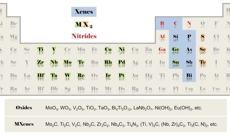
The distribution of elements of different 2-D materials. Credit: ?Science China Press
Key words: two-dimensional materials; chemical vapor deposition; heterojunctions