III–V semiconductors have preferable properties such as direct band-gaps for optoelectronics and high carrier mobility for microelectronics in comparison with Si, which is the mainstream of the semiconductor technology. Thus monolithic integration of Si with III–V semiconductors would be an attractive approach for versatile and high-performance devices.
However, large lattice mismatches between Si and III–V semiconductors have prevented the latter from high-quality epitaxial growth on Si substrates. On the nanoscale, such a problem can be circumvented owing to the efficient strain relaxation through the nanostructure surface, e.g. nanowires.
The one-dimensional growth is usually triggered by a vapor–liquid–solid (VLS) mechanism with the Au catalyst. However, possibly due to the difficulty in controlling the surface properties of Si and the chemical stability of the Au particle, a complicated pre-process for substrate is necessary for Au catalyst. As an important group in III–V family, Ga-based semiconductor nanowires could utilize Ga, which is a component itself, as the catalyst providing with a clean and compatible solution in contrast to the common Au.
Prof. ZHAO Jianhua’s research team from Institute of Semiconductors, Chinese Academy of Sciences (CAS), has done some influential work on III–V semiconductor nanostructures in recent years. Based on their earlier works on Ga-catalyzed GaAs nanowires growth on Si (YU X. Z. et al. Nano Lett. 12, 5436, 2012; Nano Lett. 13, 1572, 2013), recently, Dr. YU Xuezhe and some members in Prof. ZHAO’s team, have investigated the growth temperature dependence and effectively expanded the growth temperature window for Ga-catalyze GaAs nanowires, taking advantage of two-step approach for Ga-catalyzed GaAs nanowires growth on Si.
It is the first in-depth report on the growth temperature for Ga-catalyzed GaAs nanowires, which is a fundamental parameter for growth. Previous works were limited by the one-step approach and thus growth temperature was confined in a narrow region.
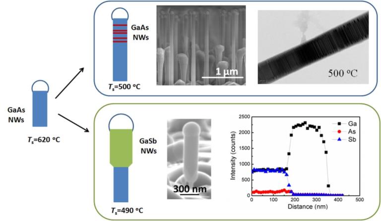
Moreover, based on above work, they have successfully fabricated GaSb/GaAs axial heterostructural nanowires on Si and also composition-tunable GaAsxSb1-x ternary nanowires by using Ga-catalyzed method.
This work could be found in the recently published Nanoscale 8, 10615, 2016 and is chosen as outside back cover for this issue. Details can be found at http://xlink.rsc.org/?DOI= C5NR07830J
This work was supported by NSFC (Youth Science Foundation), Youth Innovation Promotion Association of CAS, and MOST of China.

Figure 1. Two-step fabrication of self-catalyzed GaAs nanowires and GaAs/GaSb axial heterostructural nanowires on Si (Image by Prof. ZHAO Jianhua et al.)
Contact:
Prof. ZHAO Jianhua
E-mail: jhzhao@semi.ac.cn
Institute of Semiconductors, CAS (http://english.semi.cas.cn/)
